Saturday, July 13, 2024

Boss DR-220 Gate Array (MB670120) Interface

    I've wondered for a while how exactly the CPU of the DR-220 controls its gate array. The CPU handles the screen, buttons, and triggers. The MB670120 gate array controls ROM, RAM, and the DAC + multiplexer for playing sounds. Interestingly, the two are separated onto different boards that are joined by a pin header. This makes it very easy to separate them and experiment.

Pinout

    The service manual tells us the connections on the header, but it lists the pins in no particular order. Here they are laid out in the order they appear on the board. The signals of interest are underlined, while the others are in grey.

CPU Dir

Feature

Pin

Pin

Feature

CPU Dir

Out

OE

30

1

WR

Out

Out

CS

29

2

GND


Out

ALEL

28

3

ALEH

Out


GND

27

4

Trig-In

In


26

5


25

6


IO

B7

24

7

B6

IO

IO

B5

23

8

B4

IO

IO

B3

22

9

B2

IO

IO

B1

21

10

B0

IO

In

CLK1

20

11


GND

19

12

GND


+5V

18

13

+5V


In

CLK0

17

14

Trig-Out

Out

In

RST

16

15

CLK2

In


General Communication

    The manual also explains the mechanics of communication, but not the significance of it. The gate array determines what sounds to play based on the contents of RAM, and the CPU accesses RAM/ROM through the gate array.
    The CPU can't directly tell the gate array to do anything besides access memory for it. This means there's no instruction to "play a sound right now". Instead, it simply tells the gate array to store a specific value in a specific range of memory. A split second later, the gate array reads back the value, and plays the corresponding sound.

Timing

    The timing is provided by the manual. We're also told what signals are involved. I've redrawn the diagram here. 

MB670120 Gate Array Timing Diagram


    We have a parallel bus, but no dedicated address lines. Instead the bus is multiplexed, similar to some CPUs like the 8085. We specify a 16 bit address, one byte at a time. First the high byte is put on the bus, then the ALEH signal is brought low. This latches our values into an internal address buffer. The same is done for the low byte of that address and ALEL. The data is then put on the bus, and finally we strobe the write line. This stores a value into RAM.
    Curiously, the CPU can't read from RAM; Only the gate array can. This helps show that the RAM access is really just a way to communicate with the gate array.

Addresses

    The last bit of info that the manual gives us is the range of addresses (0-5), though it doesn't exactly say what they do. It turns out these 6 addresses correspond to 6 outputs(channels) of the multiplexer. Different samples(instruments) are hardcoded to these channels. Since we have 11 instruments, some have to strategically share channels.

Instrument

Address

BD

0000

SN

0001

LT

0002

MT

0002

HT

0002

RIM

0003

HCP

0003

OH

0004

CH

0004

RCY

0005

CCY

0005


Data

    So, what values do we put in the addresses to play sounds? The manual has no more answers.
By connecting a logic analyzer to our header, we can see the values sent to the gate array. With a little experimentation, it becomes obvious what the different values correspond to.
    A single byte per address specifies the volume, pause/play status, and instrument for the channel. That's really all we really need.


Bit Values

Effect

Bit #

7

6

5

4

3

2

1

0


Name

?

Vol2

Vol1

Vol0

Play

Inst2

Inst1

Inst0


X

X

X

X

0

X

X

X

Not Playing


X

0

0

0

1

X

X

X

Min Volume


X

1

1

1

1

X

X

X

Max Volume


X

X

X

X

1

0

0

1

Play Inst #1


X

X

X

X

1

0

1

0

Play Inst #2


X

X

X

X

1

1

0

0

Play Inst #3

  • The most significant bit appears to have no impact
  • The next 3 MSBs set the volume (The range is greater than what the CPU actually uses)
  • The next bit says if the channels should be playing or not
  • The last 3 bits specify the instrument
    There's a maximum of three instruments per channel, but 3 bits give us 8 instrument values. Unfortunately, the unused combinations don't yield any interesting results. You'll simply get one of the normal sounds for the channel, not a combination or a hidden sound.

Wrapping up

    Now that we have the pinout, protocol, memory map, and packet structure, we can play some drums! The bus is parallel, the speed is relatively slow, and the timing is forgiving, so most old CPUs should have no problem talking to the gate array. Newer microcontrollers should have it easy too, besides coming up with a dozen outputs. Since we're using the bus in only one direction, we can use a shift register to get extra outputs.
    Now we can interface anything an arduino can be connected to. This opens up the machine immensely, given that it started with only a trigger in/out. MIDI would be an easy choice, but the sky is the limit.

Sunday, June 23, 2024

Radel Tanpura schematic

     A friend was generous and patient enough to lend me his Radel Tanpura (tambura) so I could reverse engineer it. 

The Mainboard

    The mainboard is pretty straightforward. It uses a 555 as a clock to feed a johnson counter. Outputs of the counter are tapped to serve as triggers for four voices. The voices are also built around 555 timers. At the end of the audio chain is a filter with speaker amplifier.

Mainboard schematic

The Daughterboard


    In between the oscillators and the filter is a curious daughterboard. It's a hybrid integrated circuit similar to the cards of a Roland Juno-106. It's also potted in some kind of epoxy, and had to be soaked in acetone before reverse engineering. Here it is with most of the orange coating removed.

Daughterboard PCB


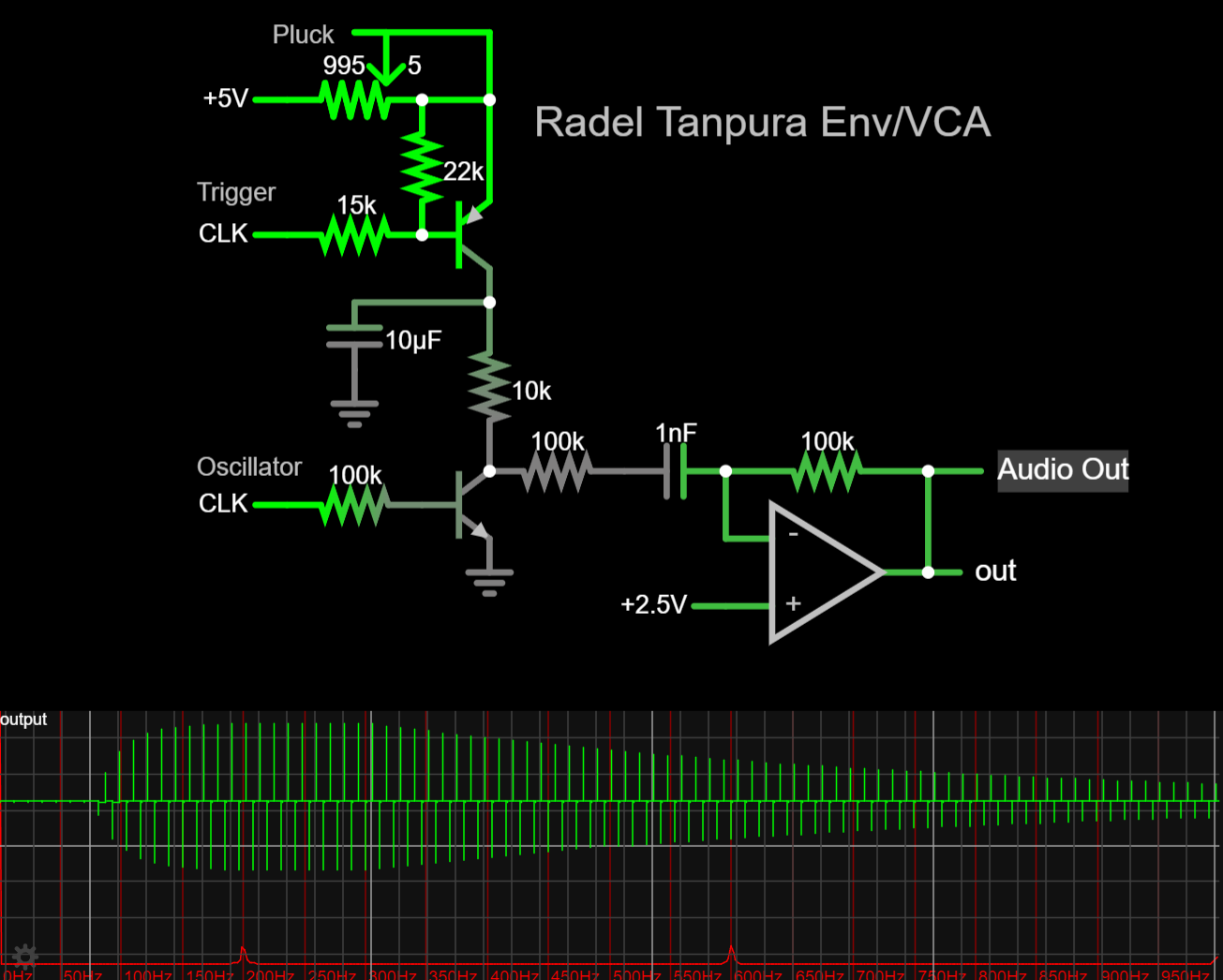
       Here's a schematic I drew from tracing the board, and probing for values. It turns out that it provides envelopes and VCAs.

Daughterboard schematic


    The PNP transistors charge the external electrolytic capacitors when they get triggers from the mainboard. The rate that they charge is controlled by a potentiometer labeled "pluck". A more conventional term for it would be "attack", as this is an envelope generator.
    The NPNs work as very crude VCAs. They pass the envelope voltage through when the oscillator is low, and they clamp the output to ground when the osc is high. This only really works because our oscillators are square waves. Other waveforms would be distorted.

    The outputs are unipolar, "reaching up" from ground. They need to be balanced equally around a reference voltage. This is achieved with the four capacitors on the board. They're part of four highpass filters that remove the DC offsets, along with other low frequencies.

    Here's a link to a Falstad simulation. You can listen to the output by allowing it to buffer, then clicking on the "Play Audio" button.


Recreation


    I used the schematics I drew to make a small clone of the instrument. I took some liberties, but it's mostly faithful. I made four daughterboards, one for each voice (osc, env, vca). Here's a short demo.
    

    I had some ideas about other ways the circuit could be implemented. Instead of highpassing the signal to make it bipolar, a portion of the envelope could be subtracted from the audio. Here's an example of the concept:

Balancing without filtering


    Some further reading and audio (of a similar model) is available at MatrixSynth courtesy of Loscha.

Saturday, April 27, 2024

Electro Harmonix EH400 Mini Synthesizer

 A friend asked me about adding CV and gate inputs to an Electro Harmonix EH400 Mini Synthesizer. Don't get it confused with their "Micro Synthesizer", "Micro Synth",  "Mono Synth", "Synth 9", etc.

I couldn't find all that much about the synth, or how to mod it, but there is a low quality scan of the schematic. It's hard to make out, and the layout obscures what the parts of the circuit are.

Original schematic

Of course I redrew it in Eagle CAD. I broke the circuit down into logical parts, laid them out in a more conventional way and labeled some signals.


Redrawn schematic

The Oscillator

The oscillator uses a single comparator and is based on a classic relaxation oscillator.
A comparator-based hysteretic oscillator - Wikipedia

It has some tweaks though. The osc can be turned on and off by applying a gate signal to D2. This is needed because there is no VCA; the oscillator has to be turned off to prevent it from droning.
The octave can be changed by toggling switch S1. It changes the configuration of the two timing caps from parallel to series. This gives a 2 octave difference between the positions.
The addition of D1 keeps the timing caps from being charged up by the R4/R5 voltage divider through R3 and R2. Instead, they're charged by an external voltage that goes through R1 and R2.

The Keyboard

This brings us to the CV generation circuit. The lefthand side of the circuit lets the user dial in a voltage that will be put through the keyboard's chain of resistors (represented by one resistor labeled "KEYBOARD"). This voltage sets the maximum pitch, and allows for tuning and pitch bend.
It's worth noting that the keyboard is made of metal foil and doesn't have conventional, mechanical keys.
When a "key" is pressed, the KEYBOARD-C node will connect to a node on the resistor ladder. This will send current through the intonation trimmer and on to the oscillator, charging the timing capacitors.
Pressing a key also puts a voltage across C4 where it can be seen by comparator IC1C. It gets compared to a divided version of the voltage that was put into the keyboard. Due to the divider, C4's voltage will always be the more positive signal when a key is being pressed. This generates a gate signal at the comparator's output.


The LFO and PWM

The LFO is based on the same circuit as the main oscillator, not that anyone would be able to tell from the original schematic. They call it "phasing", but it's really accomplishing pulse width modulation by comparing the LFO with the main osc.
The "phasing" adjustment is an odd one. It changes the switching points of the LFO. This changes both the period and amplitude of the LFO. The actual rate that the timing cap charges/discharges stays the same though (in terms of voltage/time).
If the switch is toggled, it stops being an LFO and instead delivers a constant CV. The potentiometer now adjusts this voltage, and the comparator acts like a crude unity-gain buffer.


Here are both switch states modeled separately. Falstad doesn't like to simulate the right one at high speeds and it results in the capacitor draining some before the comparator notices. This happens to turn it back into an oscillator.


The Filter

The original's filter looks especially tangled and odd. It makes more sense once you see that R29 and R37 form a voltage divider that's used as a reference voltage. That said, it's still odd.

There are two stages to the filter and they're in parallel. They have the same topology, but are tuned differently (C8/C10 vs C12/C15). Switch S5 can be used to disconnect the lower stage, and boost the upper one.

Both stages are built around CA3094 OTAs. These chips are typical OTAs that include a darlington pair that acts as a buffer. One unique feature is that all three terminals of the pair are exposed at pins 1, 8 and 6.


Here's the Falstad simulation. The buffer design is based off of the CA3094's datasheet.


The Envelope

The envelope is interesting because it uses a start and stop voltage instead of amount/offset. Unfortunately, it doesn't perform very well (at least in the simulation).
Q1 should be applying the start voltage to C6 when the gate signal is low, but C6 is always influenced somewhat by the stop voltage via R21.
When the gate is high, the start voltage is disconnected, and gives the stop voltage full control.
C6 is buffered by Q4 and sent to the current control pins of the filter stages.

There's also a piezo disc that generates a voltage when the keyboard is played forcefully. It gets buffered by Q3 and Q2 before being tied directly to the envelope's capacitor.


Leftovers

Maybe later I'll get into adding the CV control that started this. The simple answer is to add an exponential current source in place of the keyboard resistor ladder. I suspect that the oscillator's sluggish reset will cause the tuning to go flat at higher pitches though. 
It looks like a gate signal can be applied across C4 to recreate the signal from the keyboard.

The suboscillator is uninteresting as it's a simple d-type latch that's set up as a divider. The square output of the oscillator feeds into one half of the latch that seems to be used as a buffer, before going into the divider half.

There's also a 6V regulator built around a zener diode and a buffer transistor.

Lastly there's a speaker amplifier that isn't drawn, because it's not relevant to the synthesis.

Update

Revised files, including a board layout, have been added to github here.

Sunday, March 10, 2024

Korg Monotron Oscillator Sync

    I developed this mod specifically for the Montron Duo, so that one oscillator could sync to the other. Since all three models of Monotron share the same oscillator design though, the mod is applicable to them all. Here we'll look at the original model.

    The crux of syncing is resetting an oscillator, but not every oscillator lends itself to being reset. I also wanted to avoid heavily modifying the Monotron board. That means limiting things like cutting traces, lifting legs, removing/replacing components.

    Here's the VCO we have to work with, taken from the Monotron schematic. It's a saw-core that uses a couple schmitt triggers and a transistor for the charging phase, plus a current sink for the discharge phase. Q2 is constantly discharging the timing capacitor, C11. Meanwhile, the schmitts watch the voltage of C11. When it gets too low, they recharge it through Q5. The built-in thresholds of the schmitts define when they start and stop this recharging stage. 

    This "recharge" is a method of resetting. So, the oscillator already has an internal reset signal and reset mechanism.

Monotron VCO

Korg's Sync Circuit

    We need look no further than the LFO to find an actual sync circuit (though they call it "reset"). The LFO is essentially the same as the main oscillator, just with this sync circuit added.

Monotron LFO with sync circuit highlighted

    I've created a version of the LFO in Falstad's Circuit Simulator, link here. I've renamed the input to "Sync", and the internal pulse to "Reset Pulse" on the trace below.

    When the sync pulse goes high, Q8 pulls the input of the first schmitt low, as if the capacitor's charge was low. This forces the circuit into the recharge stage. Q7 pulls the second schmitt low, and delays the recharge until the sync pulse goes low. This is enough to sync the LFO.

Simulated LFO

    While this is promising, there is a catch. The reset circuit inserts resistors R33 + F1 before schmitt one, and R32 between the schmitts. This would require some fiddly trace cutting if we were to apply it to the VCO.

My Sync Circuit


    I took a different approach, and tried to discharge the capacitor using the sync pulse. This can be done with just an NPN transistor. We have to be careful about how much we discharge the capacitor though. A naive approach might discharge the cap below the point that it should begin charging again, changing the pitch and amplitude.

    We can prevent this overshoot by checking the output of the second schmitt. While it's high, we're safe to discharge. Once it goes low, we've hit the lower threshold, and it's time to stop. If we AND this signal with our sync pulse, we can safely limit how much the capacitor will discharge. We also get a free sync enable/disable input if we use a three-input AND.

New sync circuit


    This works well in practice, but there are limitations. 

    If the sync pulse is too long, it will extend past the capacitor recharging stage, and force it low again. This will keep it cycling rapidly until the sync pulse stops, and produce a high pitched tone.
    If the sync pulse is too short, the capacitor won't fully discharge before the pulse ends, and the oscillator won't reset.
    So, the ideal length for the sync pulse would be exactly long enough to discharge the capacitor.

    Keep in mind that the capacitor is always being discharged based on an ever-changing pitch voltage. The capacitor will also be charged to an arbitrary voltage when we try to reset it. This means that the discharge time is a moving target, and there is no one perfect sync pulse length.

    We can fix this by adding a set-reset latch that will catch the edge of the sync pulse, stretch it out to the right length, and end it once the capacitor is fully discharged. Here's an exaggerated trace to demonstrate the concept.

Latched sync pulse example


Here's is the Falstad link for the latched version

Latched sync circuit


    The sync pulse sets the latch, which starts discharging the capacitor. Once it discharges to the lower limit, the second schmitt will go high, resetting the latch, and allowing the capacitor to recharge.
While the non-latched circuit might be good enough, this circuit will work across a much broader range of frequencies.

Monday, February 19, 2024

Korg Monotron Duo modifications

    I've been experimenting with Monotrons since around the time of the original's release. I took an interest in the Duo model more recently though. The extra oscillator opens up some modulation options, and paraphonic possibilities. I thought it would be fun to digitally control as many parameters as possible. 

    After experimenting with using OTAs to control things, I determined that digital potentiometers would be easier. Unfortunately, there has been an ongoing shortage with the digipots that the project calls for. Because of this, the project has been shelved for some time. While working on this, I developed some modifications that don't require digipots though: 

  • Oscillator sync
  • XOR ringmod
  • Squarewave anding
  • Sub oscillator
  • PWM 
  • filter HP input
  • VCF crossmod

    I'm posting now to at least keep the schematics from sitting on my hard drive. I hope to follow this up with a breakdown of each mod.


Full schematic


Thursday, March 2, 2023

VTech Precomputer 1000 schematic

 I stumbled across the VTech Precomputer 1000, learned that it's based on a z80, and looked for a schematic. I couldn't find one, so I took a crack at drawing one myself. I haven't validated it, and there are some things still to figure out, so consider it a rough starting point.


Friday, February 17, 2023

DrumFire DF500 Schematic

    Here's one more analog drum schematic that I've redrawn. I worked from the drawing found here, and changed the layout for clarity.