#define strobe 3 //PORTD#define clk 4#define data 2void setup() {DDRD = 1 | (1<<strobe) | (1<<clk); // NES outputs}void pulse_pin(byte pin, byte del) {PORTD |= (1<<pin); //setdelayMicroseconds(del);PORTD &= ~(1<<pin); //cleardelayMicroseconds(del);}void loop() {byte btns = 0;pulse_pin(strobe, 10); //latch the controllerfor(int i = 0; i < 8; i++) { //read 8 bitsbtns = btns << 1 | !(PIND & (1<<data));pulse_pin(clk, 10); //clock next bit}// atari output d12-d8, open collectorDDRB = (btns & 0xf) | (!!(btns & 0xc0) << 4); // dpad + A||B}
Sunday, June 21, 2020
DIY NES to Atari Controller Adapter
I wanted to use my favorite NES controller with my controller-less Atari 65XE and 130XE. The NES controller uses a shift register, while the Atari expects 5 simple buttons. I wrote a simple Arduino program to convert one to the other. Using an Arduino mini, it fits in this little inline enclosure.
Thursday, June 11, 2020
DIY 1702a Programmer
I've resumed working on the PAiA 8700 computer. It uses some very old, and hard to program EPROMs: 1702As. They require +37V, +47V, +59V and ground to program.
I've come up with a relatively easy to build DIY programmer. It doesn't require a parallel port, or dozens of transistors. It's Arduino based, and uses mostly common parts.
Here's what it looks like:

And here's a schematic:

A boost converter daughter board is used to generate a high voltage, over 60V. It then gets regulated down to the various voltages needed. IC1 (TL783) has to be calibrated to +47V, then the other voltages will fall into place.
An Arduino nano is able to manipulate the high voltages through three ULN2003 transistor arrays, and one IRF520 MOSFET.
Right now the code is very crude, but functional. It's on pastebin here. The binary for the 1702A is included in the Arduino program. On power up/reset the programming sequence begins. It's finished when the pin 13 led stops flashing.
I've come up with a relatively easy to build DIY programmer. It doesn't require a parallel port, or dozens of transistors. It's Arduino based, and uses mostly common parts.
Here's what it looks like:

And here's a schematic:

A boost converter daughter board is used to generate a high voltage, over 60V. It then gets regulated down to the various voltages needed. IC1 (TL783) has to be calibrated to +47V, then the other voltages will fall into place.
An Arduino nano is able to manipulate the high voltages through three ULN2003 transistor arrays, and one IRF520 MOSFET.
Right now the code is very crude, but functional. It's on pastebin here. The binary for the 1702A is included in the Arduino program. On power up/reset the programming sequence begins. It's finished when the pin 13 led stops flashing.
I've now added the Eagle CAD files to my github here.
Pollard Syndrum Schematic Redraw
The original Syndrum schematic isn't the most legible in terms of quality or layout.
I redrew it so that it made more sense to me. Here it is:
Friday, May 22, 2020
Boss DR-110 Clap Pulse Generator (trigger adapter)
Here's a circuit I came up with a while back. I had a DR-110 with a dead digital board. The digital board is responsible for generating all the triggers in the system, and it generates some very specific triggers for the clap circuit.
CPI is three 1ms long pulses, every 10ms (100hz).
CPII is a separate pulse also 1ms long, that falls 10ms later.
CPI is three 1ms long pulses, every 10ms (100hz).
CPII is a separate pulse also 1ms long, that falls 10ms later.
I re-implemented this in the following circuit.
Traces from top to bottom are CPI, CPII, and Trigger in.
The traces are from a simulation of the circuit, that you can play with in real time here.
Breaking down the circuit, we start at C8 and R11. These form a hipass filter for the incoming trigger. This ensures that long triggers will be handled the same way as short triggers.
IC6A & B are schmitt NAND gates and they form an SR latch. It is set by an incoming trigger, and is reset by the CPII pulse. The output is used to enable the generation of the CPI signal.
IC6C is the core of an oscillator that can be enable/disabled from pin 8. It works by charging and discharging C9.
R14 sets the charging rate of C9, and determines the low time between pulses.
Breaking down the circuit, we start at C8 and R11. These form a hipass filter for the incoming trigger. This ensures that long triggers will be handled the same way as short triggers.
IC6A & B are schmitt NAND gates and they form an SR latch. It is set by an incoming trigger, and is reset by the CPII pulse. The output is used to enable the generation of the CPI signal.
IC6C is the core of an oscillator that can be enable/disabled from pin 8. It works by charging and discharging C9.
R14 sets the charging rate of C9, and determines the low time between pulses.
R15 and D4 set the discharge rate, and determine the length of the pulses.
R12 & R13 help bias C9 near the threshold voltage of IC6C. This ensures that the first pulse will be close in length to the following pulses. If C8 had to charge all the way up from ground, the first pulse would be much longer.
IC7 is a counter, and is keeping track of how many pulses have been seen on CPI.
Once the end of the third pulse is counted, output QC goes high. This resets the SR latch, disabling the oscillator, and very quickly stopping the fourth trigger.
IC7 is a counter, and is keeping track of how many pulses have been seen on CPI.
Once the end of the third pulse is counted, output QC goes high. This resets the SR latch, disabling the oscillator, and very quickly stopping the fourth trigger.
Output QC is also used as our CPII signal. To limit it to 1ms in length, we use it to charge C7 through R9. After about 1ms, C7 has charged enough to trigger the CLR pin of the counter. This causes output QC to go low again and discharge C7.
So, with some simple tweaking, this circuit can generate different lengths, rates, and numbers of pulses.
Thursday, May 7, 2020
Korg Monotron Delay PCB Component Labels
Even though it's old-hat, I'd like to try modifying the Korg Monotron Delay.
Korg was nice enough to share their schematic, but not the board layout. Also, the board itself isn't labeled.
I need to know what I'm working with, so I used a multimeter, and some educated guesses to draw the following. I labeled the rough sections of the circuit, so that it's a little easier to find what you're looking for. Be warned that it's not perfect, but should be a decent starting point.
Korg was nice enough to share their schematic, but not the board layout. Also, the board itself isn't labeled.
I need to know what I'm working with, so I used a multimeter, and some educated guesses to draw the following. I labeled the rough sections of the circuit, so that it's a little easier to find what you're looking for. Be warned that it's not perfect, but should be a decent starting point.
Wednesday, April 22, 2020
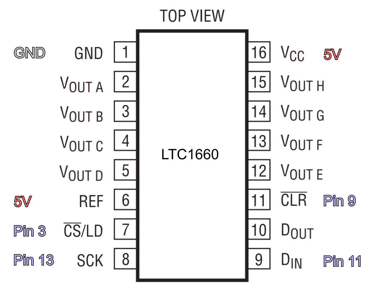
Arduino LTC1660 Octal DAC demo
I was looking for a breadboard friendly DAC with lots of outputs, and decent resolution.
I found the LTC1660. It can be had for under $10, features 8 outputs, and 10 bit resolution. This should be good enough to control VCOs over a handful of octaves.
There seems to be a single example of how to use it with an arduino, but it doesn't spell out the SPI connections. Without SPI, you're limited to slow, CPU intensive communication. With SPI, I was able to get an example program to output at around 180kHz. This will be much slower in practice, but it shows the potential of the chip.
Below are the connections and code:
#include <SPI.h> #include <stdint.h> const int pinCSLD = 3; const int pinCLR = 9; void setup() { pinMode(pinCSLD, OUTPUT); pinMode(pinCLR, OUTPUT); digitalWrite(pinCLR, HIGH); digitalWrite(pinCSLD, HIGH); SPI.begin(); SPI.setClockDivider(SPI_CLOCK_DIV2); } void loop(){ for (int i = 0; i < 1024; i++) setDAC(1, i); } void setDAC(uint16_t address, uint16_t value) { uint16_t h = address << 4 | value >> 6; uint16_t l = value << 2; PORTD &= ~(1 << pinCSLD); //LOW SPI.transfer(h); SPI.transfer(l); PORTD |= (1 << pinCSLD); //HIGH }
Saturday, April 11, 2020
Korg KR-55 Recap Guide
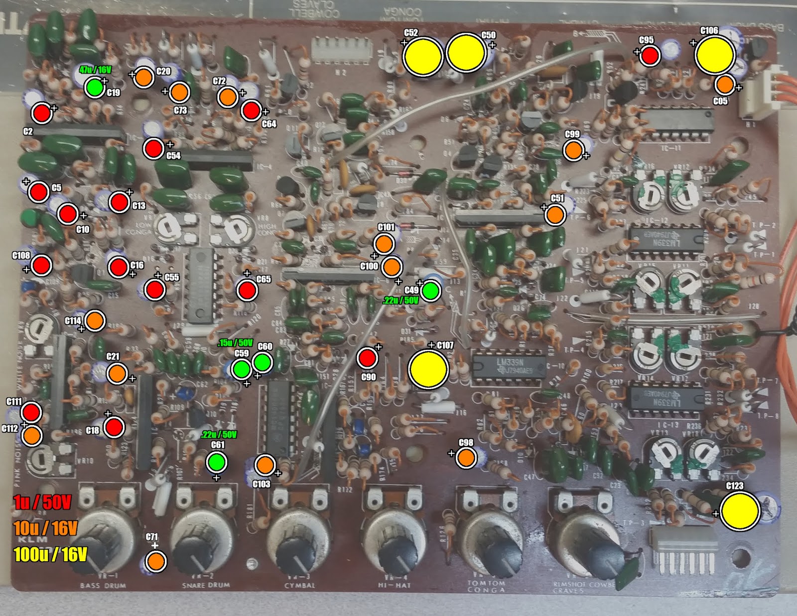
I'm repairing my second Korg KR-55 drum machine. They both had a ton of failing electrolytic capacitors that needed replacing. In the first machine, the capacitors had leaked and damaged the board. In the second, one had failed and shorted, causing the snare, hihats, and cowbell to not work.
Recommending "recaping" as a general fix, is something of meme now. It's no joke on the Korgs though. I advise replacing all the electrolytics in them, so I made a the following images and lists to help.
The logic board only has a few capacitors. The 470u are the large, axial type, and don't seem to be an issue. They're listed for completeness.
Here are the relevant capacitors on the sound board. They're color coded by value.
Red = 1u / 50V
Org = 10u / 16V
Ylw = 100u / 16V
Grn = other
Here are the footprints on the bottom, to help with desoldering. These are not coded, because they should all be removed.
Here are the individual capacitors, and their function in the circuit. This can be helpful for debugging.
Recommending "recaping" as a general fix, is something of meme now. It's no joke on the Korgs though. I advise replacing all the electrolytics in them, so I made a the following images and lists to help.
The logic board only has a few capacitors. The 470u are the large, axial type, and don't seem to be an issue. They're listed for completeness.
| Name | Value | Voltage |
| C21 | .33u | 50V |
| C1 | 10u | 16V |
| C22 | 470u | 25V |
| C23 | 470u | 25V |
Here are the relevant capacitors on the sound board. They're color coded by value.
Red = 1u / 50V
Org = 10u / 16V
Ylw = 100u / 16V
Grn = other
Here are the footprints on the bottom, to help with desoldering. These are not coded, because they should all be removed.
Here are the types and totals of capacitors:
| Value | Voltage | Total |
| .15u | 50V | 2 |
| .22u | 50V | 2 |
| 100u | 16V | 5 |
| 10u | 16V | 14 |
| 1u | 50V | 14 |
| 47u | 16V | 1 |
Here are the individual capacitors, and their function in the circuit. This can be helpful for debugging.
| Name | Value | Voltage | Role |
| C59 | .15u | 50V | Low Conga |
| C60 | .15u | 50V | Hi Conga |
| C49 | .22u | 50V | HiHat |
| C61 | .22u | 50V | Tom Noise Audio |
| C50 | 100u | 16V | Cymbal Power |
| C52 | 100u | 16V | Hat Power |
| C106 | 100u | 16V | Power |
| C107 | 100u | 16V | Power |
| C123 | 100u | 16V | Metal Power |
| C20 | 10u | 16V | Bd, Sn Power |
| C21 | 10u | 16V | Bd, Sn Power |
| C51 | 10u | 16V | Cymbal Power |
| C71 | 10u | 16V | Tom/Conga Audio |
| C72 | 10u | 16V | Tom/Conga Power |
| C73 | 10u | 16V | Tom/Conga Power |
| C98 | 10u | 16V | RS/Clav/CB Audio |
| C99 | 10u | 16V | RS/Clav/CB Power |
| C100 | 10u | 16V | RS/Clav/CB Power |
| C101 | 10u | 16V | RS/Clav/CB Power |
| C103 | 10u | 16V | Mix Audio |
| C105 (C05) | 10u | 16V | Power |
| C112 | 10u | 16V | Noise |
| C114 | 10u | 16V | Noise Power |
| C2 | 1u | 50v | Bd Trigger |
| C5 | 1u | 50v | Bd Audio |
| C10 | 1u | 50V | Sn |
| C13 | 1u | 50V | Sn Audio |
| C16 | 1u | 50V | Sn Body Audio |
| C18 | 1u | 50V | Sn Audio |
| C54 | 1u | 50V | Low Conga |
| C55 | 1u | 50V | Low Conga |
| C64 | 1u | 50V | Hi Conga |
| C65 | 1u | 50V | Hi Conga |
| C90 | 1u | 50V | Claves Audio |
| C95 | 1u | 50V | Cowbell |
| C108 | 1u | 50V | Noise |
| C111 | 1u | 50V | Noise |
| C19 | 47u | 16V | Bd, Sn Power |
Subscribe to:
Posts (Atom)