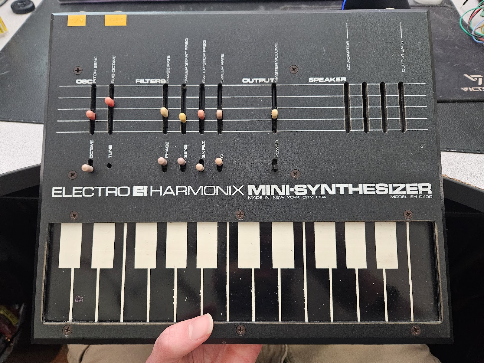
Once again we return to the EH400. This time we're looking at adding MIDI.
This mod is for a friend and needs to retain the use of the original controls. While it's tempting to build on the CV mod from last time, that's not compatible with the original touch keyboard. We need to perform the functions of the keyboard, but we have an uncommon keyboard. It works by shorting the top foil of the keyboard to one of the 25 contacts on the lower PCB. This presents one of 25 different resistances to the oscillator, and causes a note to play. How can we fake this?
Resistance
One way is to simulate this keyboard via some kind of variable resistance. It could be a digital potentiometer, or a DAC + a voltage controlled resistor. This problem is that this replaces the keyboard. This could be fixed by somehow switching between the original keyboard and the new resistance, or by reading the keyboard and using it to control the new resistance.
Push the Button
A simpler solution is to control the keyboard directly, by pretending to press the "keys". We can short the foil to the pads via some kind of switch. BJTs, optocouplers, FETs, and analog switches are among the options. Considering we'll need 25 switches, we want something that's not too cumbersome. Analog switches are nice because you can get several of them in one package. Luckily, we don't need 25 completely separate switches; they'll all be sharing the foil as one of their terminals. This means we can use an analog multiplexer like the CD4051, as it has many switches with one common connection.
One of many
It's important to pick the right multiplexer (mux) for the job. Ideally we'd find a 25:1 mux, but they really only come in powers of two, up to 16. To make things simple, we'd like it to run off of the 9V supply rail, and we'd like a low "on" resistance too. This keeps it from impacting the tuning too much. This narrows down our options to mainly derivatives of the CD4067. The 74HC4067 has a lower on resistance while still being able to tolerate the 9V supply. In practice, a normal CD4067 might be low enough though.
 |
| 4067 multiplexer |
Free range
So, we can manage our 25 switches with two muxes. There's another component to controlling the pitch though, the octave switch. It shifts the keyboard by two octaves. We'll need digital control of this octave switch in order to have the full 4 octave range available over MIDI. How does this switch work though?
Front and back, and side to side
There are two capacitors that dictate the range. One might assume that the switch selects between a larger one, and a smaller one, to change octaves. Turns out that they're both the same size though. It's their configuration that the switch changes. This is done because capacitors are somewhat low tolerance devices. Let's say they're 5%; one cap could be +5% while the other is -5%. That puts them pretty significantly out of tune with each other. Instead, the circuit uses the fact that caps in parallel sum together, and caps in series decrease in value. The math behind this turns out to work in our favor.
Parallel is simply C1 + C2, but series is (C1 * C2)/(C1 + C2). Let's plug in some worst case scenario 5% 100nf capacitors: (105nf * 95nf)/(105nf + 95nf) = 9975/200 = 49.875nf series. 105nf + 95nf = 200nf parallel. 49.875nf vs 200nf. Wow, we're only a quarter of a percent out from a perfect four-to-one relationship (two octave shift). So, this change in configuration (parallel vs serial) gives a result that brings our octaves much closer to in tune than 5% capacitors would normally allow.
Another one
We find that we need one more analog switch to control the parallel/serial capacitor configuration. This time we don't need 16 throws, but the on resistance is especially important. There are a number of candidates, but the DG409LEDY happens to be relatively cheap and available at the moment. It's a dual 4:1 mux that can handle the voltage and is rated at 17Ω on resistance.
A simple solution would be to copy the connections of the original, mechanical switch. "On resistance" wasn't a consideration in its design though. It's important that we chain as few connections through the switch as possible, so that we don't keep stacking this 17Ω penalty. Here's one arrangement that limits this while still switching between serial and parallel.
The soft side
As with any MIDI project, there's software and digital IO involved. This opens up new possibilities on a synth that was completely analog. We can control things remotely, generate new signals, or respond to new inputs. Given how spartan the synth is, there are only so many targets for modulation. The filter and the oscillator are the big ones.
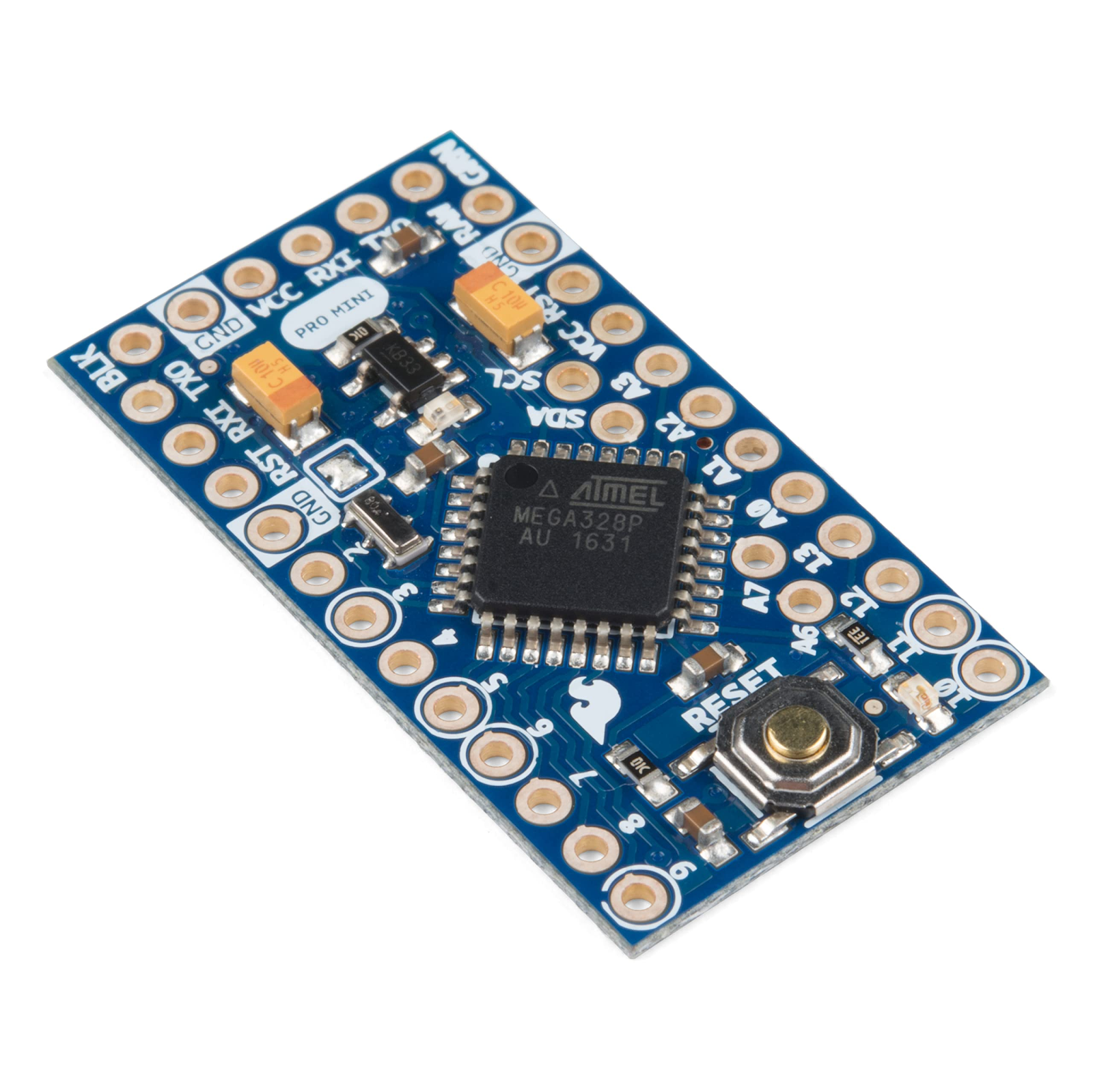 |
| Arduino Pro Mini |
Lasting impact
There's one more thing that the original keyboard offers, a form of velocity labeled "Sense". This is accomplished with a piezo that's stuck to the bottom of the keyboard, and routed into the envelope generator. We can take our MIDI velocity, turn it into a voltage, and pipe it into the same point. This is far from precise work, so we can generate our voltage in an imprecise way: pulse width modulation. Many microcontrollers have provisions to generate PWM and it can easily be filtered into a useable voltage.
Notes between notes
We can fairly easily add a feature that that original instrument lacked: portamento. This is a smooth sliding effect between notes. Just one problem, we're stuck with the rigid notes we have. But, glissando done fast enough approximates the sound of portamento. This means playing every note that falls between the previous and current note. This could be as little as zero notes, or all four octaves of notes. The effect is most convincing when done quickly and over a large range. It doesn't require any extra hardware though, just code to change notes.
Other thoughts
Key tracking could be added without too much trouble, as could other software modulation sources like LFOs, or envelopes. The only obvious destinations are the filter and the pulse width setting. These already have an envelope and an LFO respectively though.
Key retriggering could be forced on by resetting the envelope during every note on. This would disable the legato behavior of the original keyboard.
Some cross modulation would be possible with the addition of VCAs or digipots. The filter could be FM'd by the oscillator, or the oscillator could be AM'd by the LFO. At some point you lose the spirit of the original instrument though.
Closing circuit
 |
| A one-off MIDI board |
 |
| EH400 MIDI schematic |
Files
The source code and schematics for this MIDI retrofit are available on Git Hub, here. It's intended to be built with an Arduino Pro Mini, but small changes will allow it to run on many AVRs.


.png)
.png)


.png)


